opensource.google.com

Menu

El Carro for Oracle: Data migration and improved backups

Wednesday, August 10, 2022

In May 2021, we released El Carro to make it easier to run Oracle databases on Kubernetes. Our following blog dove deeper into El Carro’s features, announced support for Oracle 19c, and detailed more flexibility for building database images. Today we’re excited to open source two new features to enhance El Carro and make it easier to manage your Oracle deployments: Data Migration and Point-in-Time Recovery. Automated Data Migration makes it much easier to re-platform to El Carro and Point-in-Time Recovery is a standard feature that database professionals come to expect because it enables you to drastically reduce RPO and worry less about backup frequency.

Data Migration

The Data Migration feature of El Carro enables users to migrate data from their existing database to an El Carro database running on Kubernetes. This functionality allows users to re-platform to El Carro with minimal disruption. The two most common pathways shown in the image below are to 1) modernize in place by simply migrating your database to Kubernetes so you can leverage the automation of El Carro and to 2) migrate to Kubernetes in the cloud.
Migrate your database in place or to the cloud

Typical migration sources include AWS (RDS, EKS, EC2), Azure (AKS, VMs), GCP (GKE, GCE, BMS) or on-premises deployments. Typical migration targets include any Kubernetes installation on GCP (GKE), AWS (EKS), Azure (AKS), or on-premises.

The Data Migration feature offers two automated migration flows and two manual ones.

Category

Options

Migration Downtime

Complexity

Automated

Data Guard with physical standby

minimal

lowest

Data pump

long

low

Manual

RMAN-based migration

long

medium

Data pump

long

medium

  • Migration Downtime: required downtime to migrate source database into El Carro without data loss. Minimal means less downtime, long means more downtime.
  • Complexity: summarizes the difficulty and complexity of the migration journey.

Point-in-Time Recovery

Since its release, El Carro has provided users the ability to take backups and restore via RMAN or storage-based snapshots. Today we’re excited to release a new Point-in-Time Recovery feature to enhance El Carro’s backup functionality by automatically backing up archive redo logs to a GCS (Google Cloud Storage) bucket and allowing users to seamlessly restore their databases to any point in time within a user configurable window. This optional feature provides an additional layer of protection and enhanced restore granularity without interfering with manual backups or affecting database performance.

The diagram below contrasts the new versus old functionality. Previously, there were discrete restore points (shown in green on the top arrow) which represented limited opportunities to restore. With Point-in-Time Recovery, the entire arrow is green, meaning the recovery functionality is continuous, with restore points at any time along the green arrow.

With Point-in-Time Recovery you can restore to any point after the first backup

Conclusion

As always, you can try the open source El Carro operator for free (Apache 2.0 license) wherever you run Oracle databases. Follow the quick start guide and try out provisioning of instances, databases, users. Import data via Data Pump, manage instance parameters, choose between different methods for backups, and try out a restore. Have a look at how we integrate with external logging and monitoring solutions. Reach out via our Google group and leave feedback for what features you would like to see next, or even create your own patch, issue or pull request on GitHub.

By Kyle Meggs, Product Manager and Ash Gbadamassi, Software Engineer – Cloud Databases

GlobalFoundries joins Google’s open source silicon initiative

Wednesday, August 3, 2022

Over the last year we have been busy planning the expansion of our free open source silicon design and manufacturing program to further grow the community of developers and companies building custom silicon, and build a thriving ecosystem around open source hardware.

Today, we’re excited to announce an expansion of this program and our partnership with GlobalFoundries. Together, we're releasing the Process Design Kit (PDK) for the GlobalFoundries 180MCU technology platform under the Apache 2.0 license, along with a no-cost silicon realization program to manufacture open source designs on the Efabless platform. This open source PDK is the first result of our ongoing partnership with GF. Based on the scale and breadth of GF’s technology and manufacturing expertise, we expect to do more together to further access and innovation in semiconductor development and manufacturing.
GF180MCU 1P5M 5 metals stack-up, 9kA top metal, with MIM between M3 and M4 layers.
Google started this program with SkyWater Technologies, by releasing one of their PDKs under the Apache 2.0 license. We sponsored six shuttle runs over the course of two years, allowing the open source community to submit more than 350 unique designs of which around 240 were manufactured at no-cost.
We cannot understate the milestone that this new partnership represents in the foundry ecosystem market.

Over the past few years, the world has experienced an unprecedented acceleration of adoption of digital capabilities—driven by the pandemic, and technology megatrends that have shifted every aspect of human life. According to GlobalFoundries, this has led to roughly 73% of foundry revenue being associated with high growth markets such as mobile, IoT, and automotive. This transition has not only given rise to a “New Golden Age” of semiconductors but also a tectonic shift in how we define and deliver innovation as an industry.  

Specifically, applications using 180nm are at a global capacity of 16+ million wafers a year and bound to grow to 22+ million wafers in 2026, according to GlobalFoundries.

The 180nm application space continues to see strong market traction in motor controller, RFID, general purpose MCUs and PMIC, along with emerging applications such as IoT Sensors, Dual Frequency RFID and Motor Drive.

The collaboration between GlobalFoundries and Google will help drive innovation for the application and silicon engineers designing in these high growth areas, and is an unambiguous affirmation of the viability of the open source model for the foundry ecosystem.

The GF 180nm technology platform offers open source silicon designers new capabilities for high volume production, affordability, and more voltage options. This PDK includes the following standard cells
  • Digital standard cells libraries (7-track and 9-track)
  • Low (3.3V), Medium (5V, 6V) and High (10V) voltage devices
  • SRAM macros (64x8, 128x8, 256x8, 512x8)
  • I/O and primitives (Resistors, Capacitors, Transistors, eFuses) cells libraries
Open sourcing more PDKs is a critical step in the development of the open source silicon ecosystem:
  • Open source EDA tools can now add support for multiple process technologies.
  • Researchers can produce fully-reproducible designs against multiple technology baselines.
  • Popular open source IP blocks can be ported to different process technologies.
We cannot build this on our own, we need you: software developers and hardware engineers, researchers and undergrad students, hobbyists and industry veterans, new startups and industry players alike, to bring your fresh ideas and your proven experiences to help us grow the open source silicon ecosystem.

We encourage you to:

By Johan Euphrosine and Ethan Mahintorabi – Hardware Toolchains Team

SkyWater and Google expand open source program to new 90nm technology

Thursday, July 28, 2022

Today, Google is announcing the expansion of our partnership with SkyWater Technology. We are working together to release an open source process design kit (PDK) for SKY90-FD, SkyWater’s commercial 90nm fully depleted silicon on insulator (FDSOI) CMOS process technology. SKY90-FD is based on MIT Lincoln Laboratory’s 90 nm commercial FDSOI technology, and enables designers to create complex integrated circuits for a diverse range of applications.

Over the last two years, Google and SkyWater Technology have partnered to make building open silicon accessible to all developers, starting with the open source release of the SKY130 PDK and continuing with a series of no-cost manufacturing shuttles for developers in the open source hardware ecosystem. To date, Google has sponsored six shuttles on the Efabless platform, manufacturing 240 designs from over 364 community submissions. This is the first partnership of its type ever launched, and the results to date have been impressive.
The latest MPW-6 shuttle received 90 submissions from a diverse community across 24 different countries:

Over the coming months, we'll work closely with SkyWater Technology to release their new SKY90-FD PDK under the Apache 2.0 license and organize additional Open MPW shuttles to manufacture open source designs for this new 90nm FDSOI technology, through the Efabless platform.

We believe that having access to different technologies through open source PDKs is critical to grow and strengthen the open silicon ecosystem:

  • Developers can go beyond the constraints of their familiar process nodes and explore different performance, power and area trade offs with existing or new designs.
  • Researchers can reproduce their research on different technologies to produce diverse figures of merit.
  • Tool maintainers can generalize their technologies' backends to support more than one process.
  • The community can refine the ways we structure, distribute and maintain these PDKs.

SKY90-FD is a 90nm FDSOI process. Unlike a traditional CMOS BULK process, SKY90-FD features a thin layer of insulator material between the substrate and the upper silicon layer. This thin oxide process allows the transistor to be significantly thinner than in the BULK process, allowing the device to be “fully depleted,” and simplifying the fabrication process. This extra insulation greatly reduces parasitic current leakage and lowers junction capacitances, providing improved speed and power performance under various environmental conditions.

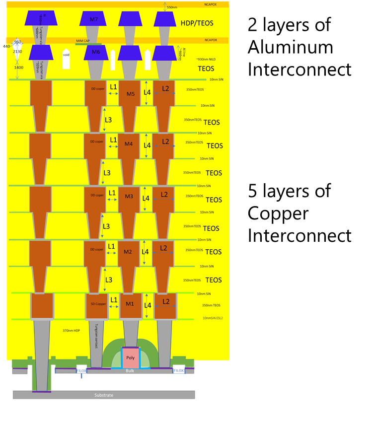
The SKY90-FD process stack topology features 5x thin Copper base metal layers for the main interconnect and two extra thicker Al (Aluminum) metal layers capable of conducting higher current.
Google is excited about the new range of applications this open source PDK will enable once it's released later this year, and we can't wait to hear from you and watch the growing stream of innovative project ideas originating from the open silicon community.

In the meantime, make sure to check https://developers.google.com/silicon for resources and pointers to start your open silicon journey!


By Johan Euphrosine and Ethan Mahintorabi – Hardware Toolchains Team

.